

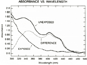
Absorbance Curves – Plot of absorbance vs. wavelength. Comparison of the absorbance of a coated photoresist film before and after exposure is used to describe a resist’s bleaching properties. The resin and photo active compound (PAC) determine the unexposed absorbance. Upon exposure, the reaction products and resin determine the absorbance of the film.
Absorption Coefficient – The fractional decrease in intensity of light passing through a material per unit distance traveled. It cannot be too high or light energy will not reach the bottom of the film.
Acid-Catalyzed Resist – A chemically amplified resist like SU-8 where an acid is produced upon exposure and this acid serves as a catalyst for a reaction during post expose bake (PEB) to change the solubility of the resist in a developer.
Adhesion – Ability of a material to adhere/bond/stick to a substrate without substantial undercut during develop or wet etch.
Actinic Wavelength – The wavelength at which a photoresist is sensitive. It is used to expose the photoresist in a lithographic system.
Additive Patterning – A process in which material is deposited in places where a pattern is to be formed. Examples are lift off and electroplating. Al has been deposited by evaporation using a lift off process. For small features, Cu is being electroplated since we are unable to plasma etch it.
Aerial Image – The 3D image of a mask pattern that is projected into the photoresist coated wafer by an optical system.
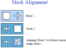
Alignment – The act of positioning (manually or automatically) the image of a specific point/target on a photomask i.e. the alignment mark, to a specific point/target on the wafer, i.e. the alignment target, to be imaged. Alignment accuracy is the overlay measured at this alignment target.
Antireflective Coating – A coating that is placed on top (TAR) or below (BARC) the layer of resist to eliminate or reduce the reflection of light and reduce the detrimental effects of standing waves or thin film interference.
Aspect Ratio – The ratio of a resist feature’s height to its width.
CD – Critical Dimension – When fabricating a device, the smallest dimension on a lithography level that must be accurately controlled to optimize electrical performance, e.g. gate dimension.
Cauchy Coefficients – The Coefficients of the Cauchy equation give an empirical expression for the variation of the index of refraction of a material as a function of wavelength (λ).
Chemically Amplified Resist – A type of photoresist, which, upon post-exposure bake (PEB), will multiply/amplify the number of chemical reactions through the use of chemical catalysis.
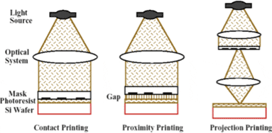
Contact Printing – A lithographic method where a photomask is placed in direct contact with a photoresist coated wafer/substrate and the pattern is transferred by exposing light through the photomask into the photoresist.
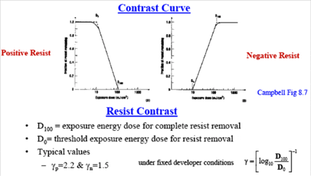
Contrast – Related to the slope of an image. The contrast, characteristic, or H-D curve is a plot of relative resist thickness remaining after development vs. the log of the exposure dose it saw. The shape of the curve is important in characterizing a resist and the lithographic process used.
Source: MIT
Dehydration Bake – A bake step performed on a wafer before coating with resist in order to remove water from the surface of the wafer surface.
Depth of Focus (DOF) – The total range of focus that can be tolerated, to keep the resulting printed feature within a variety of specifications e.g. linewidth, sidewall angle, resist loss, and exposure latitude. Increasing the NA will result in smaller patterns, but the DOF will decrease.
![]()
K2 depends on the process and criteria used to define an acceptable image.
Design Rule – A geometrical rule that defines minimum widths and/or spacings and other geometries used when laying out a mask pattern.
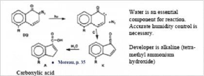
Developer – The chemical (typically a liquid) used after expose to selectively dissolve resist as a function its chemical composition. Ideally, we want a large difference in developer solubility between exposed and unexposed resist. It can be aqueous or solvent.
Dill Parameters – Three parameters, called A, B, and C, that are used in the Dill exposure model for photoresists. A and B represent the bleachable and non-bleachable absorption coefficients of the resist, respectively. C represents the first-order kinetic rate constant of the exposure reaction. It is named for Frederick Dill at IBM who first publish this model. Also, called the photoresist ABC parameters.
Direct Write Lithography – A lithography expose method whereby the pattern is written directly on the resist with e-beam, laser, ion or proton beam without the use of a mask.
Dissolution Inhibitor – A chemical which, when added to a photoresist, decreases the dissolution rate of the resist in developer. For many positive photoresists, the unexposed photoactive compound (PAC) acts as a dissolution inhibitor.
Dissolution Promoter – A chemical which, when added to a photoresist, increases the dissolution rate of the resist in developer. For many positive photoresists, the exposed photoactive compound (PAC) biproducts acts as a dissolution promoter or enhancer.
For DNQ positive photoresist, exposure produces an indene carboxylic acid which is soluble in TMAH based aqueous developer.
DNQ Photoresist – Typical g-Line and i-Line positive photoresist. Comprised of Novolak resin, diazonaphthoquinone (DNQ) photoactive compound (PAC) and solvents.
Dose to Clear (Eo) – The amount of exposure energy required to just clear the resist in a large clear area for a given process.
Dose to Size – The amount of exposure energy required to produce the proper dimension of the resist feature.
Edge Acuity – Quality of the edge of an image, determined by adhesion and shot noise
Edge Bead – A build-up of resist along the outer edge of the wafer caused by resist surface tension during the spin coating process. Removing it is important to avoid problems later in the lithography process. It can be a source of particles which reduce yield.
Etch Resistance – Ability of a material to withstand dry or wet chemical etch.
EUV Lithography – Lithography using light of a wavelength in the range of about 5nm to 50nm, with about 13nm being the most common. Also, called soft x-ray lithography.
Exposure – The process of subjecting a resist to light energy, electron, or X-ray energy for the purpose of causing chemical change in the resist.
Hg lines: g-Line(436nm) i-Line(365nm)
UV: 248nm 193nm
X-ray: 13nm – 0.4nm
Electron: 10keV – 100keV
Ions: 50keV – 200keV
Flood Exposure – Exposure of the resist to blanket radiation (all over) with no pattern. For projection tools such as a stepper, this is also called an open frame exposure (exposure with no mask or with a blank glass mask).
Focus-Exposure Matrix – The variation of resist linewidth as a function of both focus and exposure energy. The data is typically plotted as linewidth versus focus for different exposure energies and these plots are often referred to as smiley plots, spider plots, or Bossung curves.
Glass Transition Temperature (Tg) – The temperature (or the midpoint of the temperature range) at which a polymer makes a transition from behaving mostly like a solid to behaving mostly like a liquid.
Hard Bake – The process of heating the wafer after development of the resist in order to harden the resist patterns in preparation for subsequent pattern transfer. Also called postbake and post-develop bake.
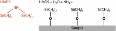
HMDS – Hexamethyldisilazane is the most widely used adhesion promotor/primer used to increase adhesion to SiO2 for DNQ type resists. It changes the SiO2 surface from hydrophilic to hydrophobic. Applied by spin coating or by vapor prime. Over priming can be counterproductive.
Wetting angle:
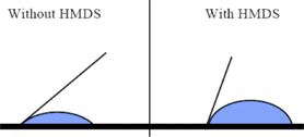
Image Reversal – A chemical process by which a positive photoresist is made to behave like a negative photoresist. Image reversal has been used to produce the reentrant profile needed for metal lift-off
Immersion Lithography – A mode of optical lithography, where an immersion fluid, with a refractive index of one or greater, fills the gap between the projection lens and the resist on a wafer. The recent interest in immersion lithography is based on the hope of improved depth of focus at a constant resolution, or improved resolution at a constant depth of focus.
Imprint Lithography – A patterning method based on embossing where a topographic (3D) pattern on a mask is replicated as a topographic pattern into a polymer film by pressing the mask (template) directly into the polymer media. Also, called nanoimprint lithography, due to the high resolution possible. The low cost and high resolution capabilities of imprint lithography make it a promising candidate for some niche applications.
Iso-Dense Print Bias – The difference between the dimensions of an isolated line and a dense line (a line inside an array of equal lines and spaces) holding all other parameters constant. Also, called Iso-Dense Bias. The iso-dense print bias is a strong function of feature size and partial coherence of the exposure system.
Lift-Off Process – A lithographic process by which the pattern transfer takes place by coating a material over a patterned resist layer, then dissolving the resist to “lift off” the material that is deposited on top of the resist. The lift-off process avoids an etch step.
Line Edge Roughness (LER) – The deviation of a feature edge, viewed top down, from a smooth, ideal shape. The edge deviations of a feature that occur on a dimensional scale much smaller than the resolution limit of the imaging tool that was used to print the feature.
One simple measure of line edge roughness is the RMS deviation of an edge from a best fit straight line.
Lithography – A method of producing three-dimensional relief patterns on a substrate. From the Greek lithos, meaning stone, and graphia, meaning to write.
Mask – A glass or quartz plate containing information about the features to be printed. Also, called a photomask or reticle.
Maskless Lithography – Any one of a number of lithographic techniques, including direct write lithography that does not use a permanent, fixed mask to perform imaging.
Metrology – The process of measuring structures on the wafer, such as the width of a printed resist feature or the overlay between two printed patterns.
Multilayer Resist (MLR) – A resist scheme by which the resist is made up of more than one layer, typically a thick conformal bottom layer under a thin imaging layer, possibly with a barrier layer in between. The need for a very thin imaging layer can be met using a mutilayer resist scheme.
Negative Photoresist – A photoresist where the areas that are exposed to light develop at a much slower rate than those areas not exposed to light.
Optical Absorption – Attenuation of light by a material.
Optical Density – Transmittance intensity to the base 10 logarithm of a material of a given thickness.
Overlay Mark – The target patterns printed on the wafer at two different litho steps that allow the overlay between the two lithography patterns to be measured.
Pellicle – A thin, transparent membrane placed above and/or below a photomask to protect the photomask from particulate contamination. Particles on the pellicle are significantly out of focus and thus have a very much reduced chance of “printing” or impacting image quality.
Photoactive Compound (PAC) – The component of a photoresist that is sensitive to light. Also called a sensitizer in a DNQ resist system.
Photoacid Generator (PAG) – The light sensitive component of a chemically amplified resist that generates an acid upon exposure to light. The resist must be baked (PEB) for the acid to allow the amplification reaction to occur and affect dissolution rate.
Pitch – The sum of the linewidth and spacewidth for a repeating pattern of long lines and spaces.
Positive Photoresist – A photoresist whose chemical structure allows for the areas that are exposed to light to develop at a faster rate than those areas not exposed to light.

Post-Exposure Bake (PEB) – The process of heating the resist coated wafer immediately after exposure in order to cause diffusion of the PAC and reduce the effects of standing waves. For a chemically amplified resist, this bake also causes a catalyzed chemical reaction that changes the solubility of the resist. Control of the temperature during the post-exposure bake is critical to linewidth control in most DUV chemically amplified resists.
Prebake – The process of heating the wafer after application (coating) of the resist in order to drive off the solvents in the resist. Also called soft bake and post-apply bake.
Process Window – A window/region made by plotting contours that correspond to various specification limits, as a function of exposure and focus. One simple process window, called the CD process window, is a contour plot of the high and low CD specifications as a function of focus and exposure. Other typical process windows include sidewall angle and resist loss. Often, several process windows are plotted together to determine the overlap of the windows to determine process latitude. One of the most useful ways of characterizing the capabilities of a lithographic process is by examining the size of its focus-exposure process window.
Tolerance to a change, e.g. +-10% in exposure dose vs. a CD change
Proximity Bake – A type of baking where the wafer is held in very close proximity to a hotplate typically on 3 pins. Proximity baking reduces the possibility of particle generation that can result from hotplate contact baking.
Quantum Efficiency – Refers to photoresist exposure. The quantum efficiency is the average number of exposure reaction products produced when one photon is absorbed by the photoreactive species.
Reflectivity – The ratio of reflected light intensity to the incident light intensity.
Refractive Index – The real part of the refractive index of a material is the ratio of the speed of light in vacuum to the speed of light in the material. The change in the refractive index of a material with wavelength is called dispersion.
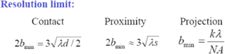
Resolution – The smallest feature of a given type that can be printed by a resist-developer and process with acceptable quality and control. Resolution is often defined as the smallest feature of a given type that meets a given depth of focus requirement. Resolution can be improved by using a lower wavelength and higher numerical aperture expose tool.
Sensitivity – It is the minimum dose needed to form a desired image on a substrate after the lithographic process. It is process dependent.
For optical positive or negative photoresists: Given in units of mJ/cm2 at a given λ (wavelength) or λ range.
For e-beam resists: Electron dose in (μC/cm2) microcoulombs per square centimeter required for the degree of electron-induced reaction to occur so a specific solvent developer will give an acceptable image. The sensitivity of PMMA scales roughly with electron accelerating voltage, with a critical dose at 50kV, for example, is about twice that of 25kV exposure.
Scanning Electron Microscope (SEM) – An instrument that is used to inspect resist profiles and measure critical dimensions by bombarding the sample with electrons and detecting the backscattering of the electrons.
Shelf Life – Time before which a resist will continue to retain specific performance parameters. Usually, lower storage temperature will extend shelf life.
Simulation – The process of using physical models to predict the behavior of a complex process. These models are usually implemented as computer software. Lithography simulation has become an essential tool for research, development and manufacturing.
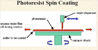
Spin Coating – The process of coating a thin layer of resist onto a substrate by dispensing a liquid resist onto the substrate and then spinning the substrate to achieve a thin uniform coat. Although apparently simple, spin coating can result in a remarkably uniform photoresist film.
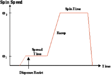
A Simple Resist Spin Coating Program:
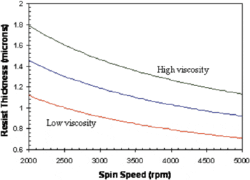
Film Thickness vs. Spin Speed for 3 Different % Solids Resists:
Standing Waves – A periodic variation of intensity as a function of depth into the resist that results from interference between a plane wave of light traveling down through the photoresist and one which is reflected up from the substrate. Standing waves are reduced by lowering the reflectivity of the substrate, increasing the absorption in the resist, or by using broadband illumination. PEB has been used to reduce standing waves in DNQ resists.
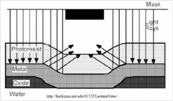
Problem is worse on metal like Al and Au.
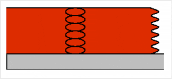
An anti-reflective coat (ARC) is used to address this problem.
Stepper – A type of projection printing tool that exposes a small portion of a wafer at one time, and then steps the wafer to a new location to repeat the exposure. Since their introduction in the late 1970s, steppers have dominated the lithographic market.
Substrate – The film stack, including the wafer, on which the resist is coated. The optical properties of the substrate and microstructures on it can have a great impact on the lithography process.
Surfactant – A “surface acting agent”, is a chemical that acts only on the surface of some material. One or more surfactants are commonly used in developers to reduce surface tension. Surface inhibition can often be induced through the use of surfactants in the developer.
TMAH – Tetramethylammonium hydroxide A 2.38% (0.26N) aqueous solution is widely used as a developer for positive photoresists.
Vapor Prime – A chemical treatment of a wafer to remove water from its surface and change the hydrophobicity prior to resist coating. HMDS is a widely used adhesion promoter. The most effective method of applying adhesion promoter is the vapor prime method.
Vector Scan – A type of direct write lithography tool where an exposing beam is not raster scanned but rather is moved directly to the area to be exposed before the beam is turned on and scanned over the exposure area. For some mask patterns, vector scan exposure tools can show much greater throughput than traditional raster scan tools.
X-ray Lithography – Lithography using light of a wavelength in the range of about 0.1nm to 5nm, with about 1nm being the most common. X-ray lithography requires the use of proximity printing since focusing elements are difficult if not impossible to produce at these wavelengths.