

Photoresists & Specialty Chemicals
Sacrificial Via Protection for TSV and MEMS Applications
Part of the Applications Notes LineThe rapid expansion of 3D-WLP (wafer-level-packaging) and MEMS is accelerating the growth of high topography features and their integration with 3D-TSV technologies. A large number of technologies have been demonstrated with the common goal to create more functionality while occupying less real-estate.
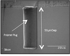
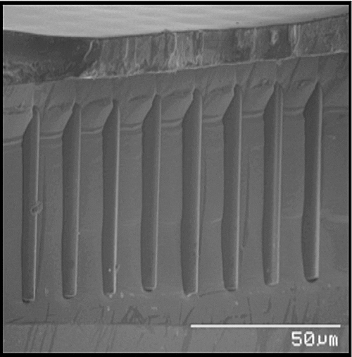
One of the preferred processes for creating deep TSVs (through-silicon-vias) is the “via first” approach. This allows the TSVs to be etched before any expensive and critical CMOS processing. This method can impact later critical process stages and as a result thick sacrificial planarizing materials can be used to create a flat starting substrate that’s pre-etched with protected TSVs. Illustrated here is the use of MicroChem via fill materials.
Benefits/Attributes
- Materials specially designed as a spin-on polymer for sacrificial TSV filling and planarization
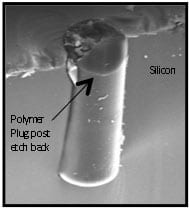
- Silicon vias protected against subsequent processes
- Easily removed using industry standard wet and dry chemistries
- Single coat with void free filling
- Thermally stable
- Options for etch back process, wet, dry or CMP.
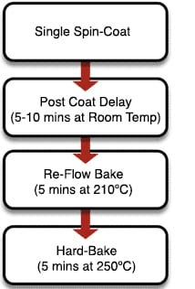
Process Flow
Strip Rate

Source:: MCC / University of Durham Technical Poster
FEATURED APPLICATIONS