

StructSure™
Photoresists & Specialty Chemicals
Photoresists & Specialty Chemicals
PermiNex® 1000 and 2000 Wafer Bonding Adhesives
Part of the StructSure™ LineKayaku Advanced Materials, Inc. PermiNex® 1000 and 2000 resists are epoxy based, photo-imageable bonding resist used as an adhesive layer for the definition and capping of cavity structures such as BAW, SAW, microfluidic devices, and others, where critical alignment, low temperature processing and high bond quality are desired.
Material Attributes:
|
Resolution Capability
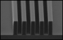
5µm features in 15µm thick PermiNex® 1000
Source: Kayaku Advanced Materials
Bonding Capability
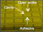 Test cavity structures |
 Adhesive cavity wall |
|
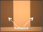
| Si to Glass bonded wafers, 10µm thick PermiNex® adhesive structure Source: Kayaku Advanced Materials |
||
LEARN MORE>
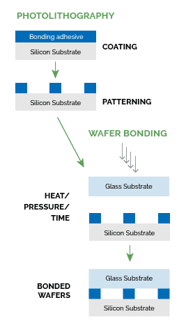
Overall Process Flow
FEATURED APPLICATIONS